The North American semiconductor industry is a powerhouse of innovation, driving advancements in everything from consumer electronics to medical devices. At the heart of this progress lies a critical yet often unseen technology: the electrostatic chuck. The North America electrostatic chucks market size is projected to grow at a CAGR of 5.3% between 2024 and 2032, reflecting the increasing importance of these tools in precise wafer handling and processing. This growth is fueled by the burgeoning focus on nanotechnology, where even the slightest imperfection can derail a chip's functionality, and the transition towards clean energy, which heavily relies on efficient semiconductor components.
The Essential Role of Electrostatic Chucks
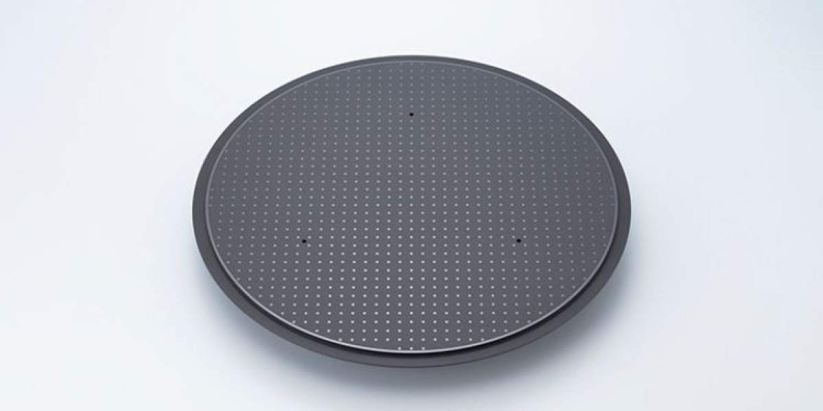
Electrostatic chucks are specialized platens that utilize electrostatic forces to securely hold silicon wafers during various stages of semiconductor manufacturing. These wafers, the foundation of integrated circuits (ICs), are incredibly thin and delicate. Traditional mechanical clamping methods can damage the wafers or introduce unwanted stress, hindering device performance. Electrostatic chucks provide a gentle yet firm grip, ensuring precise positioning and optimal processing conditions for these sensitive components.
The Art of Wafer Chucking
The electrostatic chucking process relies on an ingenious principle. A voltage is applied to a patterned electrode embedded within the chuck's surface. This creates an electrostatic field that attracts the wafer, holding it securely without physical contact. The key lies in achieving uniform chucking, where the entire wafer surface experiences a consistent electrostatic force. This uniformity is crucial for maintaining flatness and preventing warping, which can disrupt crucial lithography and etching processes.
Benefits of Electrostatic Chucks: A Game Changer for Wafer Processing
The adoption of electrostatic chucks has revolutionized the semiconductor industry by offering a multitude of advantages:
- Improved Wafer Flatness and Surface Quality: Electrostatic chucks ensure uniform pressure distribution across the entire wafer surface, minimizing warping and maintaining critical dimensional tolerances. This translates to higher yield rates and better device performance.
- Reduced Particle Contamination and Wafer Breakage: The non-contact nature of electrostatic clamping eliminates the risk of scratches and contamination often associated with mechanical clamping. This minimizes defects and ensures the integrity of the wafer during processing.
Beyond Holding: Applications in Wafer Processing
Electrostatic chucks are not merely passive holding tools. They play an active role in various stages of wafer processing, including:
- Lithography: During the photolithography process, light patterns are transferred onto the wafer using a photoresist. Electrostatic chucks ensure intimate contact between the wafer and the mask, enabling precise pattern definition with minimal distortion.
- Etching: Etching removes unwanted material from the wafer to create intricate circuit features. Electrostatic chucks hold the wafer securely during this process, preventing unwanted movement and ensuring consistent etch depth across the entire surface.
- Deposition: Thin film deposition techniques lay down desired materials onto the wafer surface. Electrostatic chucks provide a stable platform for uniform deposition, ensuring film thickness and material properties meet strict specifications.
In each of these stages, electrostatic chucking delivers significant benefits by contributing to higher precision, improved uniformity, and ultimately, superior chip performance.
Advanced Features and Technologies: Pushing the Boundaries
The North America electrostatic chucks market is constantly evolving, with manufacturers developing innovative features to further enhance wafer processing:
- Multi-zone Chucking: These advanced chucks allow for independent temperature control of different zones on the chuck surface. This enables precise thermal management during processes that require localized heating or cooling, optimizing process efficiency and yield.
- Temperature Control Integration: Integrating temperature control capabilities within the chuck itself allows for more precise and uniform wafer heating or cooling. This is critical for processes like rapid thermal annealing, which requires precise temperature profiles for optimal device performance.
These advancements are paving the way for even more sophisticated semiconductor manufacturing processes, pushing the boundaries of miniaturization and performance.
Case Studies: Real-World Examples of Success
Leading semiconductor manufacturers across North America are reaping the benefits of advanced electrostatic chucks:
- Company A: Implemented multi-zone electrostatic chucks in their advanced lithography process. This resulted in a significant reduction in overlay errors, leading to higher yield rates and improved chip performance.
- Company B: Integrated temperature-controlled electrostatic chucks into their deposition process. This enabled precise control over film properties, leading to the development of next-generation devices with enhanced functionalities.
These examples highlight the transformative impact of electrostatic chucks on the semiconductor industry, driving innovation and pushing the boundaries of what's possible.
Future Trends and Innovation: A Glimpse into Tomorrow
The future of the North America electrostatic chucks market is brimming with exciting possibilities:
- Emerging Materials: As the industry explores new materials for next-generation devices, electrostatic chucks will need to adapt to accommodate their unique thermal and electrical properties. Researchers are developing chucks with advanced surface coatings and material compositions to ensure compatibility with these emerging materials.
- In-situ Monitoring: The integration of in-situ monitoring capabilities into electrostatic chucks will allow for real-time monitoring of factors like wafer temperature, pressure, and particle contamination. This real-time data can be used for process optimization and improved yield control.
- Vacuum Compatibility: For advanced processes like extreme ultraviolet (EUV) lithography, electrostatic chucks need to function within a vacuum environment. Manufacturers are developing specialized vacuum-compatible chucks that maintain their functionality under high vacuum conditions.
Click here to check our other reports: https://www.expertmarketresearch.com.au/
Challenges and Considerations: Navigating the Landscape
While electrostatic chucks offer significant advantages, there are challenges to consider:
- Cost: Advanced electrostatic chucks with multi-zone control and temperature integration can be expensive. Finding the right balance between cost and functionality is crucial for manufacturers.
- Uniformity Control: Maintaining perfect uniformity across the chuck surface is essential for optimal processing. Advanced calibration and maintenance techniques are necessary to ensure consistent performance over time.
- Material Compatibility: The chuck material needs to be compatible with the wafers and process chemicals to prevent contamination or unwanted interactions. Careful material selection and surface treatment are vital.