In the bustling heart of California's Silicon Valley, where innovation thrives, a hidden hero plays a pivotal role in the creation of the electronic marvels we depend on daily. This unsung hero is the probe card, a critical tool in the semiconductor industry, responsible for ensuring the functionality of every microchip produced. We will delve into the fascinating world of Probe Card Design in California, uncovering the intricacies of this technology and the creative minds behind its evolution.
What is a Probe Card?
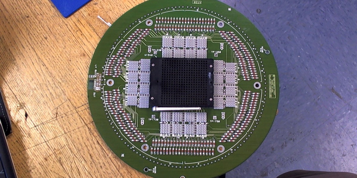
A probe card is a vital component in the semiconductor manufacturing process, specifically in the testing phase. It serves as a bridge between the semiconductor wafer, which contains numerous microchips, and the testing equipment. Essentially, it facilitates the process of testing each chip's electrical functionality before they are integrated into electronic devices.
The Importance of Accurate Testing:
Accurate testing of semiconductor wafers is crucial in ensuring that only fully functional chips make their way into consumer electronics, aerospace systems, medical devices, and beyond. Any defective chips that slip through the testing process can lead to product failures, safety hazards, and significant financial losses for manufacturers.
Evolution of Probe Card Design:
· Early Beginnings
The history of probe cards dates back to the early days of semiconductor manufacturing. In the mid-20th century, when the first integrated circuits were being developed, engineers and scientists recognized the need for a reliable means of testing these minuscule marvels. This realization gave birth to the rudimentary probe cards of yesteryears.
· Technological Advancements
Fast forward to the present day, and probe card design has evolved into a sophisticated field. California, as a hub for technological innovation, has played a pivotal role in pushing the boundaries of what probe cards can achieve. Engineers and designers in the state have consistently pushed the envelope, developing cutting-edge technologies to meet the demands of modern semiconductor manufacturing.
· Miniaturization and Precision
One of the most remarkable aspects of probe card design in California is the relentless pursuit of miniaturization and precision. As semiconductor technology has advanced, the components being tested have become smaller and more intricate. Probe cards have had to keep pace, with designers constantly refining their designs to accommodate these shrinking dimensions.
The Creative Minds Behind Probe Card Design:
· The Engineers
At the heart of probe card design are the engineers. These brilliant minds work tirelessly to develop innovative solutions to the ever-evolving challenges of semiconductor testing. Their expertise lies in the fields of electrical engineering, materials science, and precision mechanics.
· The Materials Experts
Materials play a pivotal role in probe card design. California's abundance of research institutions and high-tech companies has allowed materials scientists to experiment with cutting-edge materials. These experts search for materials that offer the perfect balance of conductivity, durability, and thermal stability to ensure the probe card functions flawlessly under extreme conditions.
· The Innovators
Innovation is the lifeblood of California's tech industry, and probe card design is no exception. Innovators in this field constantly seek novel approaches to improve the efficiency and accuracy of semiconductor testing. Their creativity has led to breakthroughs in probe card technology that have reverberated throughout the electronics industry.
Key Challenges in Probe Card Design:
· Thermal Management
One of the most significant challenges in probe card design is managing the extreme temperatures generated during semiconductor testing. As chips become more powerful, they generate more heat, which can affect the accuracy of the testing process. Engineers in California have developed advanced cooling solutions to address this issue.
· Contact Density
With semiconductor components becoming smaller and denser, maintaining precise contact with each chip's testing points is a formidable challenge. Probe card designers have risen to the occasion by developing advanced micro-probing technologies that can access these ultra-tiny contact points with pinpoint accuracy.
· Longevity and Reliability
Probe cards are subjected to rigorous testing conditions and must endure millions of probe cycles without failure. Ensuring their longevity and reliability is an ongoing challenge. California-based companies invest heavily in research and development to create robust probe cards that can withstand the rigors of semiconductor testing.
The Future of Probe Card Design:
· Artificial Intelligence Integration
As artificial intelligence continues to make inroads into the semiconductor industry, probe card designers are exploring ways to integrate AI algorithms into the testing process. This promises to enhance testing efficiency and accuracy, reducing the likelihood of defects in semiconductor products.
· 3D Stacking Technology
The advent of 3D stacking technology presents new opportunities and challenges for probe card design. This technology allows multiple semiconductor layers to be stacked on top of each other, increasing chip density. Probe cards will need to evolve to accommodate this vertical integration while maintaining their precision.
· Sustainable Design
In an era of increasing environmental consciousness, probe card designers in California are also focusing on sustainable materials and manufacturing processes. This includes developing Probe Cards that can be reused or recycled, reducing waste in
Conclusion
In the world of semiconductor manufacturing, Probe Cards are the unsung heroes, silently ensuring the quality and reliability of the electronic devices we rely on every day. In California, a hotbed of innovation, probe card design has reached new heights, with engineers, materials scientists, and innovators pushing the boundaries of what is possible.
As semiconductor technology continues to advance, so too will the art of probe card design. With challenges like thermal management, contact density, and longevity to conquer, California's creative minds are well-equipped to shape the future of this essential industry.
In the heart of California's Silicon Valley, probe card designers remain dedicated to their craft, ensuring that the electronic devices of tomorrow will be more powerful, reliable, and sustainable than ever before. So, the next time you pick up your smartphone or use any electronic device, remember the unsung heroes of probe card design, working diligently behind the scenes to make it all possible.